This is an old revision of the document!
Table of Contents
Default Firmware
The ZTEX SDK includes Default Firmwares for all Series 2 FPGA Boards. They define a set of compatible features:
- Bitstream uploading to volatile and non-volatile memory
- Communication interface:
- Hi-speed bi-directional interface operating at maximum possible data rate of the hardware
- Low speed communication with SRAM like interface (e.g. useful to transfer settings)
- 4 GPIO pins
- 1 dedicated reset pin
- Host Software API and HDL modules for FPGA
- Update utility DefaultUpdater detects FPGA Board and automatically installs latest Default Firmware.
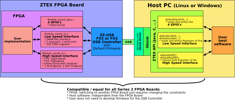
The feature-rich communication interface makes firmware development obsolete in may cases, e.g. most examples of the SDK use default firmwares. Because all functions are compatible the host software can be made board independent.
A more detailed overview is given by the following block diagram
HDL Modules
There are 3 HDL modules which are located in directory default/fpga-fx[2|3]/ of the SDK:
| Module Name | Description | Used in this examples |
|---|---|---|
ezusb_io.v | bi-directional high-speed interface | memfifo |
ezusb_lsi.v | SRAM like low speed interface | ucecho |
ezusb_gpio.v | GPIO's and reset signal | memfifo, ucecho |
ezusb_io.v
This module implements the high-speed communication for both directions using the EZ-USB Slave FIFO interface (FX2) or GPIF2 (FX3). It provides the following features:
- buffering and filtering of the interface clock from the EZ-USB
- High-speed input using slave FIFO interface / GPIF2 of the EZ-USB FX2/FX3
- High-speed output using slave FIFO interface / GPIF2 of the EZ-USB FX2/FX3
- Scheduler if both directions are active
- shared EZ-USB ↔ FPGA bandwidth: 96 MByte/s (FX2) or 208 MByte/s (FX3)
- usable host ↔ FPGA bandwidth: 30..35 MByte/s (USB 2.0) or 200..207 MByte/s (FX3 in USB 3.0 mode)
- short packet support using 'PKTEND'
The interface is compatible for all FPGA Boards and listed below. A brief description is given in the comments. The hardware pins are omitted because they depend from the EZ-USB variant and are directly connected to the interface of the top level module. In order to learn more about the usage please take a look into the top level module of the memfifo examle.
module ezusb_io (
        output ifclk,
        input reset,                    // asynchronous reset input
        output reset_out,		// synchronous reset output
        // pins
        input ifclk_in,
        inout [15:0] fd,
	output reg SLWR, SLRD,	        // low active
	output reg SLOE, PKTEND,	// low active
	input EMPTY_FLAG, FULL_FLAG,	// almost full/empty due to flag latency of several clocks, low active
// signals for FPGA -> EZ-USB transfer
        input [15:0] DI,                // data written to EZ-USB
        input DI_valid,			// 1 indicates data valid; DI and DI_valid must be hold if DI_ready is 0
        output DI_ready, 		// 1 if new data are accepted
        input DI_enable,		// setting to 0 disables FPGA -> EZ-USB transfers
    	input pktend_arm,		// 0->1 transition enables the manual PKTEND mechanism:
    	                                // PKTEND is asserted as soon output becomes idle
    	                                // recommended procedure for accurate packet transfers:
    	                                //   * DI_valid goes low after last data of package
    	                                //   * monitor PKTEND and hold DI_valid until PKTEND is asserted (PKTEND = 0)
        input [15:0] pktend_timeout,	// automatic PKTEN assertion after pktend_timeout*65536 clocks of no output data
    					// setting to 0 disables this feature
	// signals for EZ-USB -> FPGA transfer
        output reg [15:0] DO,           // data read from EZ-USB
        output reg DO_valid,		// 1 indicated valid data
        input DO_ready,			// setting to 1 enables writing new data to DO in next clock; DO and DO_valid are hold if DO_ready is 0
    					// set to 0 to disable data reads
        // debug output
        output [6:0] status
    );
ezusb_lsi.v
This module is intended for low speed communication, such as transfer of configuration data.It has an easy-to-use SRAM like interface and is used in the ucecho example. Particular features are:
- SRAM-like interface
- 1 read port, 1 write port
- 256 32 Bit registers
The user-interface is the same for both EZ-USB variants. Only the hardware pins depends on type of FPGA-Board and are omitted here (copy it from the examples). A short description is given in the comments.
// all directions are seen from FPGA
module ezusb_lsi (
	// control signals
	input clk,			// at least 24MHz
	input reset_in,			// high-active asynchronous reset
	output reg reset,	        // synchronous reset output
	// hardware pins
        // ...
	// user interface
	output reg [7:0] in_addr,	// input address
	output reg [31:0] in_data,	// input data
	output reg in_strobe,     	// 1 indicates new data received (1 for one cycle)
	output reg in_valid,    	// 1 if data is valid
	output reg [7:0] out_addr,      // output address
	input [31:0] out_data,          // output data
	output reg out_strobe	        // 1 indicates new data request (1 for one cycle)
    );
ezusb_gpio.v
The default interface implements 4 freely usable and independent bidirectional GPIO pins. It is used in the memfifo examle. The user interface is independent from FPGA board and listed an described (see the comments) below. Just the hardware pins differ (omitted below).
// all directions are seen from FPGA
module ezusb_gpio (
	// control signals
	input clk,			// system clock, minimum frequency is 24 MHz
	// hardware pins
        // ...
	// interface
	output reg [3:0] in,	        // inputs
	input [3:0] out			// wired-OR outputs: GPIO's not used for output must be 0
    );
Device Identification
Default Firmware has several configurable properties which can be used to identify devices, e.g. if several FPGA Boards are running on the same host.
All of them can be set using FWLoader.
| Property | FWLoader parameter |
|---|---|
| USB vendor ID (must be purchased from USB IF) and product ID | -su <VID> <PID> |
| Product name | -sp <string> |
| Custom serial number (up to 10 characters) | -ss <sn string> |
| Default unique serial number stored in MAC EEPROM | -ss 0000000000 |
