Table of Contents
Memory tutorial for USB-FPGA-Modules 1.15
This tutorial explains how the memory controller IP Core is created on USB-FPGA-Modules 1.15.
Creating the IP Core
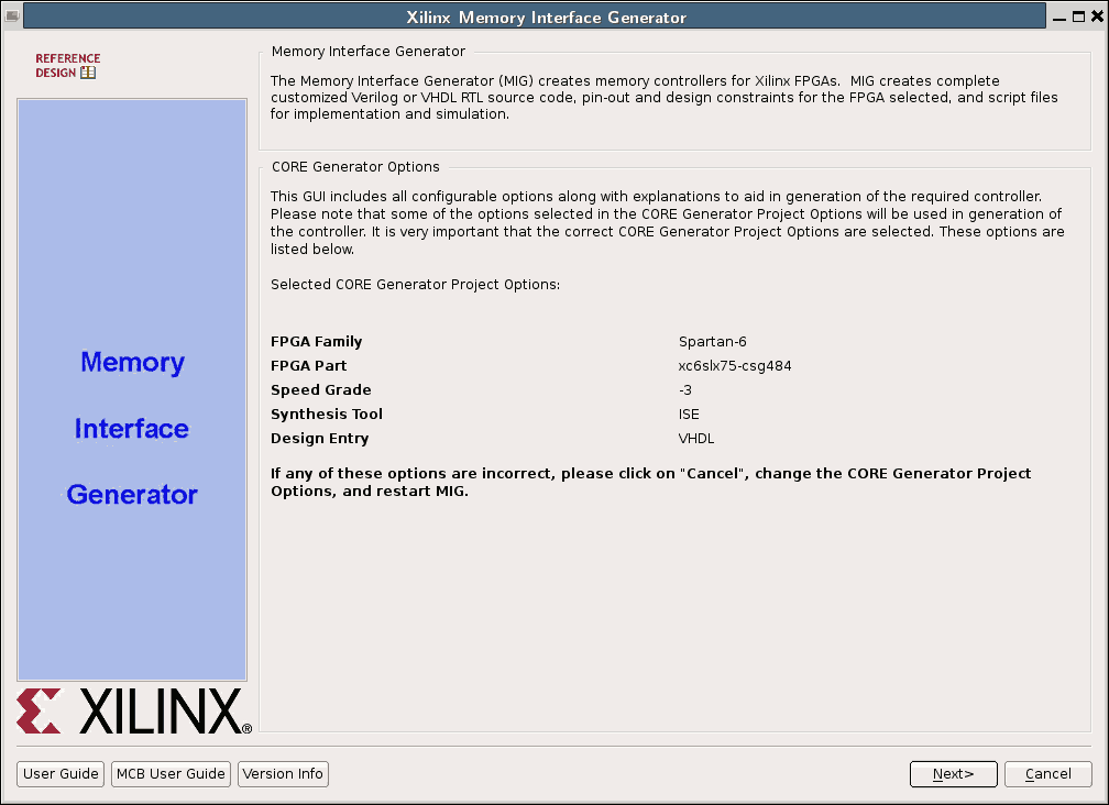
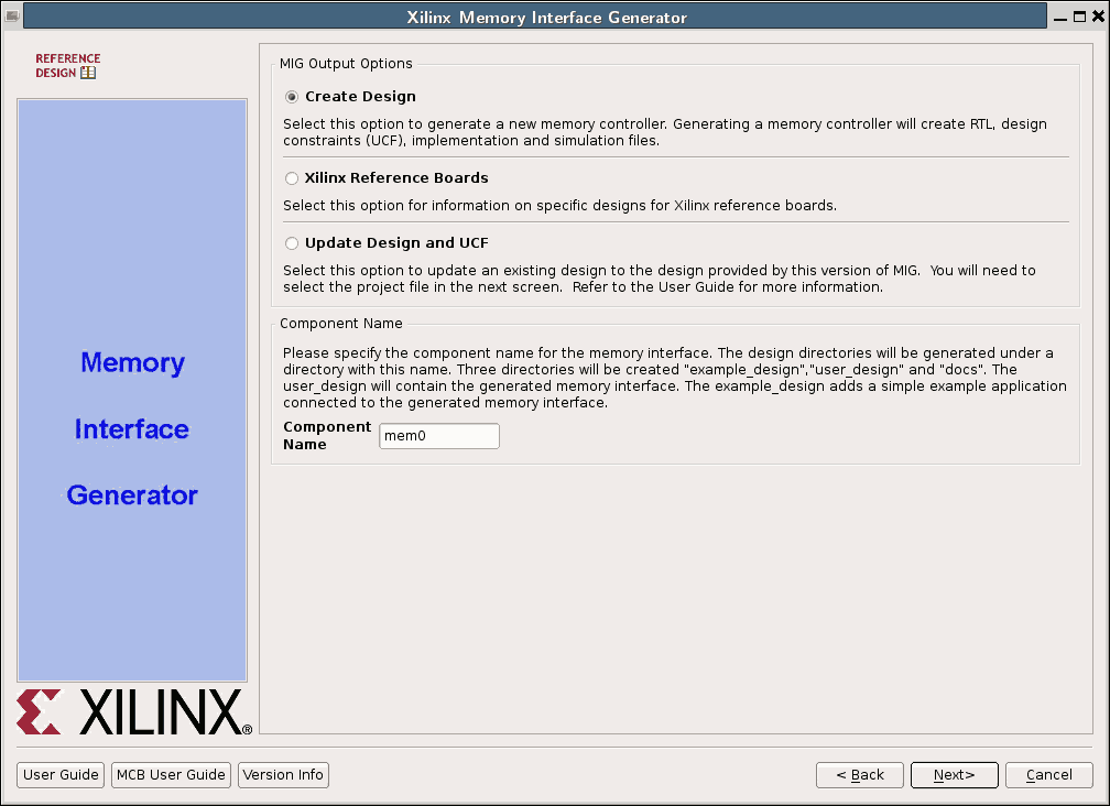
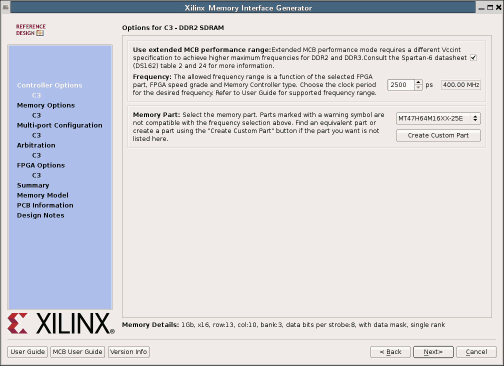
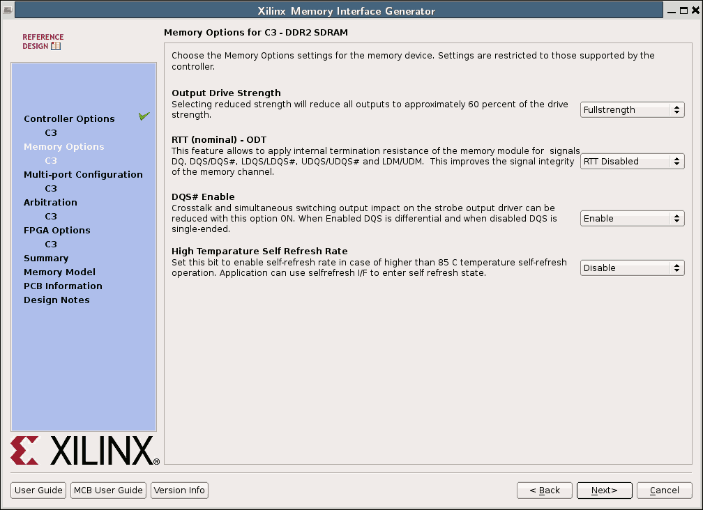
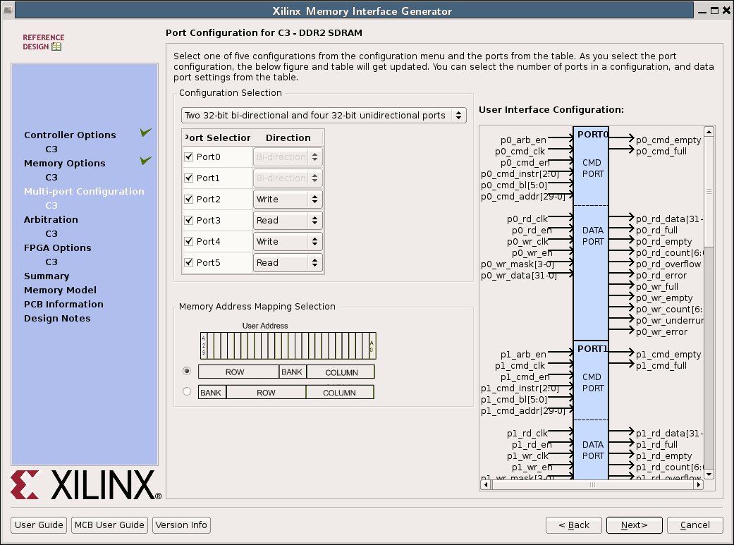
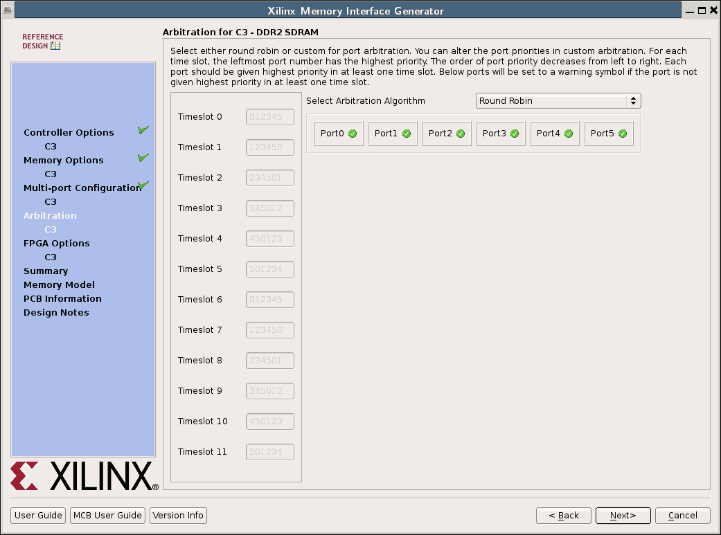
This section describes how the IP Core is created in an ISE project. The MIG version used for the screen shots below was MIG 3.5 (of ISE version 12.2). The settings for other versions should be very similar.
- In the menu:
Project→New Source - Choose
IP Core Generatorand enter a name for the new Core - Select
Memories & Storage Elements→Memory Interface Generators→MIGand click onNEXT→FINISH - Click
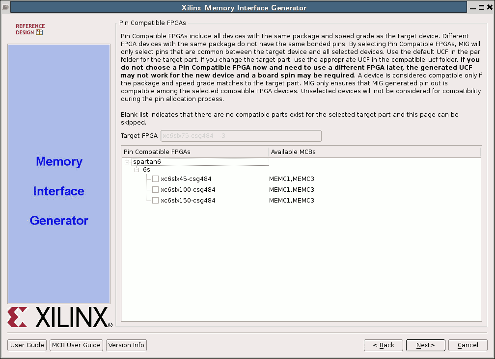
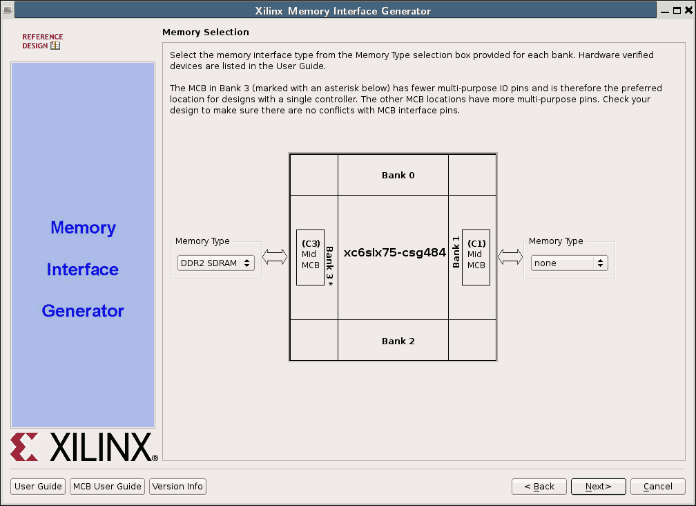
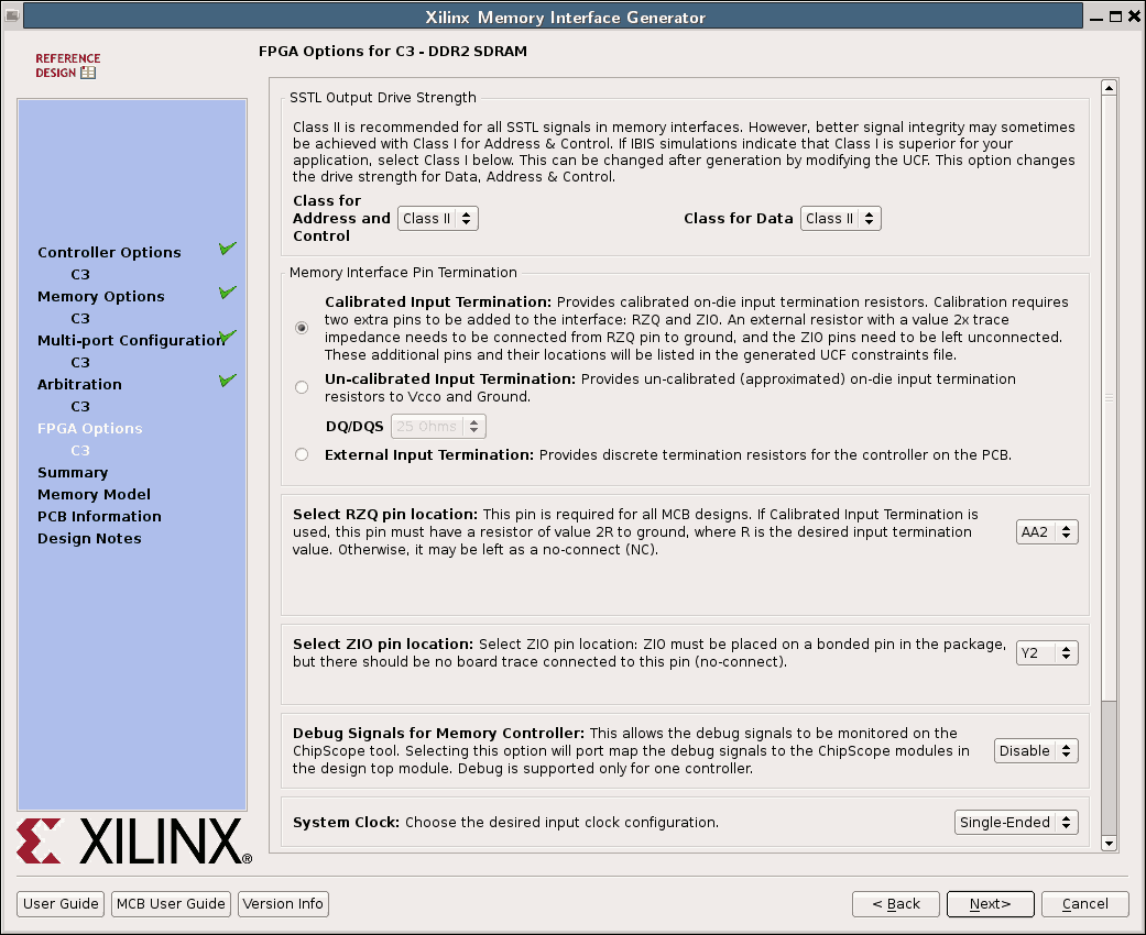
NEXTon the following dialog boxes andGenerateon the last screen.
Modify your .ucf file
Insert the following code snippet into your ucf file
NET "FXCLK" TNM_NET = "FXCLK";
TIMESPEC "TS_FXCLK" = PERIOD "FXCLK" 20.83333 ns HIGH 50 %;
NET "FXCLK"  LOC = "L22" | IOSTANDARD = LVCMOS33 ;


############################################################################
## Memory Controller 3
## Memory Device: DDR_SDRAM->MT46V32M16XX-5B-IT
## Frequency: 400 MHz
## Time Period: 2500 ps
## Supported Part Numbers: MT46V32M16BN-5B-IT
############################################################################
CONFIG MCB_PERFORMANCE= EXTENDED;

############################################################################
## I/O TERMINATION
############################################################################
NET "mcb3_dram_dq[*]"                                 IN_TERM = NONE;
NET "mcb3_dram_dqs"                                   IN_TERM = NONE;
NET "mcb3_dram_dqs_n"                                 IN_TERM = NONE;
NET "mcb3_dram_udqs"                                  IN_TERM = NONE;
NET "mcb3_dram_udqs_n"                                IN_TERM = NONE;

NET  "mcb3_dram_a[*]"                                 OUT_TERM = UNTUNED_50;
NET  "mcb3_dram_ba[*]"                                OUT_TERM = UNTUNED_50;
NET  "mcb3_dram_ck"                                   OUT_TERM = UNTUNED_50;
NET  "mcb3_dram_ck_n"                                 OUT_TERM = UNTUNED_50;
NET  "mcb3_dram_cke"                                  OUT_TERM = UNTUNED_50;
NET  "mcb3_dram_ras_n"                                OUT_TERM = UNTUNED_50;
NET  "mcb3_dram_cas_n"                                OUT_TERM = UNTUNED_50;
NET  "mcb3_dram_we_n"                                 OUT_TERM = UNTUNED_50;
#NET  "mcb3_dram_odt"                                  OUT_TERM = UNTUNED_50;
NET  "mcb3_dram_dm"                                   OUT_TERM = UNTUNED_50;
NET  "mcb3_dram_udm"                                  OUT_TERM = UNTUNED_50;

############################################################################
# I/O STANDARDS
############################################################################
NET  "mcb3_dram_dq[*]"                               IOSTANDARD = SSTL18_II;
NET  "mcb3_dram_a[*]"                                IOSTANDARD = SSTL18_II;
NET  "mcb3_dram_ba[*]"                               IOSTANDARD = SSTL18_II;
NET  "mcb3_dram_dqs"                                 IOSTANDARD = DIFF_SSTL18_II;
NET  "mcb3_dram_udqs"                                IOSTANDARD = DIFF_SSTL18_II;
NET  "mcb3_dram_dqs_n"                               IOSTANDARD = DIFF_SSTL18_II;
NET  "mcb3_dram_udqs_n"                              IOSTANDARD = DIFF_SSTL18_II;
NET  "mcb3_dram_ck"                                  IOSTANDARD = DIFF_SSTL18_II;
NET  "mcb3_dram_ck_n"                                IOSTANDARD = DIFF_SSTL18_II;
NET  "mcb3_dram_cke"                                 IOSTANDARD = SSTL18_II;
NET  "mcb3_dram_ras_n"                               IOSTANDARD = SSTL18_II;
NET  "mcb3_dram_cas_n"                               IOSTANDARD = SSTL18_II;
NET  "mcb3_dram_we_n"                                IOSTANDARD = SSTL18_II;
#NET  "mcb3_dram_odt"                                 IOSTANDARD = SSTL18_II;
NET  "mcb3_dram_dm"                                  IOSTANDARD = SSTL18_II;
NET  "mcb3_dram_udm"                                 IOSTANDARD = SSTL18_II;
NET  "mcb3_rzq"                                      IOSTANDARD = SSTL18_II;
NET  "mcb3_zio"                                      IOSTANDARD = SSTL18_II;

############################################################################
# MCB 3
# Pin Location Constraints for Clock, Masks, Address, and Controls
############################################################################
NET  "mcb3_dram_a[0]"                            LOC = "M5" ;
NET  "mcb3_dram_a[10]"                           LOC = "K6" ;
NET  "mcb3_dram_a[11]"                           LOC = "B1" ;
NET  "mcb3_dram_a[12]"                           LOC = "J4" ;
NET  "mcb3_dram_a[1]"                            LOC = "L4" ;
NET  "mcb3_dram_a[2]"                            LOC = "K3" ;
NET  "mcb3_dram_a[3]"                            LOC = "M4" ;
NET  "mcb3_dram_a[4]"                            LOC = "K5" ;
NET  "mcb3_dram_a[5]"                            LOC = "G3" ;
NET  "mcb3_dram_a[6]"                            LOC = "G1" ;
NET  "mcb3_dram_a[7]"                            LOC = "K4" ;
NET  "mcb3_dram_a[8]"                            LOC = "C3" ;
NET  "mcb3_dram_a[9]"                            LOC = "C1" ;
NET  "mcb3_dram_ba[0]"                           LOC = "E3" ;
NET  "mcb3_dram_ba[1]"                           LOC = "E1" ;
NET  "mcb3_dram_ba[2]"                           LOC = "D1" ;
NET  "mcb3_dram_cas_n"                           LOC = "P3" ;
NET  "mcb3_dram_ck"                              LOC = "F2" ;
NET  "mcb3_dram_ck_n"                            LOC = "F1" ;
NET  "mcb3_dram_cke"                             LOC = "J6" ;
NET  "mcb3_dram_dm"                              LOC = "H1" ;
NET  "mcb3_dram_dq[0]"                           LOC = "N3" ;
NET  "mcb3_dram_dq[10]"                          LOC = "R3" ;
NET  "mcb3_dram_dq[11]"                          LOC = "R1" ;
NET  "mcb3_dram_dq[12]"                          LOC = "U3" ;
NET  "mcb3_dram_dq[13]"                          LOC = "U1" ;
NET  "mcb3_dram_dq[14]"                          LOC = "V2" ;
NET  "mcb3_dram_dq[15]"                          LOC = "V1" ;
NET  "mcb3_dram_dq[1]"                           LOC = "N1" ;
NET  "mcb3_dram_dq[2]"                           LOC = "M2" ;
NET  "mcb3_dram_dq[3]"                           LOC = "M1" ;
NET  "mcb3_dram_dq[4]"                           LOC = "J3" ;
NET  "mcb3_dram_dq[5]"                           LOC = "J1" ;
NET  "mcb3_dram_dq[6]"                           LOC = "K2" ;
NET  "mcb3_dram_dq[7]"                           LOC = "K1" ;
NET  "mcb3_dram_dq[8]"                           LOC = "P2" ;
NET  "mcb3_dram_dq[9]"                           LOC = "P1" ;
NET  "mcb3_dram_dqs"                             LOC = "L3" ;
NET  "mcb3_dram_dqs_n"                           LOC = "L1" ;
#NET  "mcb3_dram_odt"                             LOC = "M3" ;
NET  "mcb3_dram_ras_n"                           LOC = "N4" ;
NET  "mcb3_dram_udm"                             LOC = "H2" ;
NET  "mcb3_dram_udqs"                            LOC = "T2" ;
NET  "mcb3_dram_udqs_n"                          LOC = "T1" ;
NET  "mcb3_dram_we_n"                            LOC = "D2" ;

# The following pins are available for used as RZQ or ZIO pins#
NET  "mcb3_rzq"                                  LOC = "AA2" ;
NET  "mcb3_zio"                                  LOC = "Y2" ;
Insert the Core into your VHDL code
Please use memtest.vhd from the memory test example as reference.
- Add the following inputs/outputs to the entity declaration:
FXCLK         : in std_logic;
RESET_IN      : in std_logic;

-- DDR2-SDRAM
mcb3_dram_dq     : inout std_logic_vector(15 downto 0);
mcb3_rzq         : inout std_logic;
mcb3_zio         : inout std_logic;
mcb3_dram_udqs   : inout std_logic;
mcb3_dram_udqs_n : inout std_logic;
mcb3_dram_dqs    : inout std_logic;
mcb3_dram_dqs_n  : inout std_logic;
mcb3_dram_a      : out std_logic_vector(12 downto 0);
mcb3_dram_ba     : out std_logic_vector(2 downto 0);
mcb3_dram_cke    : out std_logic;
mcb3_dram_ras_n  : out std_logic;
mcb3_dram_cas_n  : out std_logic;
mcb3_dram_we_n   : out std_logic;
--mcb3_dram_odt    : out std_logic;
mcb3_dram_dm     : out std_logic;
mcb3_dram_udm    : out std_logic;
mcb3_dram_ck     : out std_logic;
mcb3_dram_ck_n   : out std_logic
- Add the component declaration from
ipcore_dir/<ipcore name>.vhoto the architecture header. - Define the following signals in the architecture header:
signal CLK : std_logic;         -- 50 MHz system clock (for example)
signal RESET0 : std_logic;	-- released after dcm0 is ready
signal RESET : std_logic;	-- released after MCB is ready
signal MEM_CLK : std_logic;     -- memory clock
signal C3_CALIB_DONE : std_logic;
signal C3_RST0 : std_logic;
- Insert the instantiation template from
ipcore_dir/<ipcore name>.vhointo the architecture body and connect the following component ports:mcb3_dram_dq => mcb3_dram_dq, mcb3_dram_a => mcb3_dram_a, mcb3_dram_ba => mcb3_dram_ba, mcb3_dram_ras_n => mcb3_dram_ras_n, mcb3_dram_cas_n => mcb3_dram_cas_n, mcb3_dram_we_n => mcb3_dram_we_n, --mcb3_dram_odt => mcb3_dram_odt, mcb3_dram_cke => mcb3_dram_cke, mcb3_dram_ck => mcb3_dram_ck, mcb3_dram_ck_n => mcb3_dram_ck_n, mcb3_dram_dqs => mcb3_dram_dqs, mcb3_dram_dqs_n => mcb3_dram_dqs_n, mcb3_dram_udqs => mcb3_dram_udqs, -- for X16 parts mcb3_dram_udqs_n=> mcb3_dram_udqs_n, -- for X16 parts mcb3_dram_udm => mcb3_dram_udm, -- for X16 parts mcb3_dram_dm => mcb3_dram_dm, mcb3_rzq => mcb3_rzq, mcb3_zio => mcb3_zio, c3_sys_clk => MEM_CLK, c3_sys_rst_n => RESET0, c3_clk0 => open, c3_rst0 => C3_RST0, c3_calib_done => C3_CALIB_DONE,
The signals CLK, RESET0 and MEM_CLK are defined in the next section.
Setup the clock resource
On ZTEX USB-FPGA Modules 1.15 the memory clock is generated from the 48 MHz output clock of the EZ-USB. Unfortunately the memory interface generator (MIG) expects that the memory clock comes from an external pin (at least up to version 3.5). The common case that the clock is generated from another clock is ignored by the MIG.
In order to support internal generated clocks a few lines of the memory controller block (MCB) interface generated by the MIG have to be modified.
There are two possibilities to generate the memory clock:
- The memory clock is generated by an additional DCM instance.
- The PLL instance used to generate the internal clocks required by the MCB is modified and the 48 MHz clock is directly used as input clock. This requires no additional clock resources.
Both solutions described below defined a system clock CLK.
Memory clock generation using a DCM
This approach is used in the memtest examples.
- Insert the following statements before the entity declaration.
Library UNISIM;
use UNISIM.vcomponents.all;
- Define the following signals in the architecture body:
signal DCM0_LOCKED : std_logic;
signal DCM0_CLK_STATUS :  std_logic_vector(2 downto 1);
- Insert the DCM instantiation into the architecture body. For SG2 FPGA's (e.g. USB-FPGA Module 1.15a)
CLKFX_MULTIPLYmust be set to21:inst_dcm0 : DCM_CLKGEN generic map ( CLKFXDV_DIVIDE => 8, -- modify if other CLK than 50 MHz is desired CLKFX_DIVIDE => 3, CLKFX_MULTIPLY => 25, -- 400 MHz memory clock, SG3 @ extended voltage range -- CLKFX_MULTIPLY => 21, -- 336 MHz memory clock, SG2 CLKFX_MD_MAX => 0.0, CLKIN_PERIOD => 20.833333, SPREAD_SPECTRUM => "NONE", STARTUP_WAIT => FALSE ) port map ( CLKFX => MEM_CLK, -- 400 MHz = 48 MHz / CLKFX_DIVIDE * CLKFX_MULTIPLY CLKFX180 => open, CLKFXDV => CLK, -- can be used as system clock, 50 MHz = MEM_CLK / CLKFXDV_DIVIDE LOCKED => DCM0_LOCKED, PROGDONE => open, STATUS => DCM0_CLK_STATUS, CLKIN => FXCLK, FREEZEDCM => '0', PROGCLK => '0', PROGDATA => '0', PROGEN => '0', RST => RESET_IN );
- Add the following statement to the architecture body (right after the instantiations):
RESET0 <= RESET_IN or (not DCM0_LOCKED) or DCM0_CLK_STATUS(2);
- Apply the changes / patch listed below to to
ipcore_dir/<ipcore name>/user_design/rtl/memc3_infrastructure.vhd, i.e. remove all global input buffer (IBUFG) stuff and replaceCLKIN1 ⇒ sys_clk_ibufgbyCLKIN1 ⇒ sys_clkThis allows to connect an internally generated clock to the input of the PLL instance used for the generation of MCB clocks. The .diff file can be found in the memtest example asipcore_dir/mem0/user_design/rtl/memc3_infrastructure.vhd.diff.--- memc3_infrastructure.orig.vhd 2010-08-20 11:42:53.000000000 +0200 +++ memc3_infrastructure.vhd 2010-08-20 11:48:07.000000000 +0200 @@ -122,7 +122,6 @@ signal mcb_drp_clk_bufg_in : std_logic; signal clkfbout_clkfbin : std_logic; signal rst_tmp : std_logic; - signal sys_clk_ibufg : std_logic; signal sys_rst : std_logic; signal rst0_sync_r : std_logic_vector(RST_SYNC_NUM-1 downto 0); signal powerup_pll_locked : std_logic; @@ -135,7 +134,6 @@ attribute KEEP : string; attribute max_fanout of rst0_sync_r : signal is "10"; attribute syn_maxfan of rst0_sync_r : signal is 10; - attribute KEEP of sys_clk_ibufg : signal is "TRUE"; begin @@ -144,33 +142,6 @@ pll_lock <= bufpll_mcb_locked; mcb_drp_clk <= mcb_drp_clk_sig; - diff_input_clk : if(C_INPUT_CLK_TYPE = "DIFFERENTIAL") generate - --*********************************************************************** - -- Differential input clock input buffers - --*********************************************************************** - u_ibufg_sys_clk : IBUFGDS - generic map ( - DIFF_TERM => TRUE - ) - port map ( - I => sys_clk_p, - IB => sys_clk_n, - O => sys_clk_ibufg - ); - end generate; - - - se_input_clk : if(C_INPUT_CLK_TYPE = "SINGLE_ENDED") generate - --*********************************************************************** - -- SINGLE_ENDED input clock input buffers - --*********************************************************************** - u_ibufg_sys_clk : IBUFG - port map ( - I => sys_clk, - O => sys_clk_ibufg - ); - end generate; - --*************************************************************************** -- Global clock generation and distribution --*************************************************************************** @@ -209,7 +180,7 @@ ( CLKFBIN => clkfbout_clkfbin, CLKINSEL => '1', - CLKIN1 => sys_clk_ibufg, + CLKIN1 => sys_clk, CLKIN2 => '0', DADDR => (others => '0'), DCLK => '0',
Memory clock generation by modification of the MCB PLL
It is not possible to generate a 400 MHz clock from 48 MHz within the PLL constraints, i.e. only non-standard clocks can be generated with this method.
- Add the following interconnection to the memory core instantiation:
c3_clk0 => CLK,
- Add the following statement to the architecture body (right after the instantiations):
RESET0 <= RESET_IN;
MEM_CLK <= FXCLK;
- Modify
ipcore_dir/<ipcore name>/user_design/rtl/memc3_infrastructure.vhd- Around line 114: Set the value for
CLK_PERIOD_NStoconstant CLK_PERIOD_NS : real := 20.8333333;
- Around line 155: Modify the following clock dividers / multipliers of the u_pll_adv instantiation as desired (examples can be found below):
CLKOUT0_DIVIDE     => C_CLKOUT0_DIVIDE,    -- memory clock * 2
CLKOUT1_DIVIDE     => C_CLKOUT1_DIVIDE,    -- memory clock * 2
CLKOUT2_DIVIDE     => C_CLKOUT2_DIVIDE,
CLKOUT3_DIVIDE     => C_CLKOUT3_DIVIDE,
...
DIVCLK_DIVIDE      => C_DIVCLK_DIVIDE,     -- valid values for 48 MHz input clock: 1 and 2
CLKFBOUT_MULT      => C_CLKFBOUT_MULT,
Example 1: 396 MHz memory clock
CLKOUT0_DIVIDE     => 1,    -- 792 MHz, memory clock * 2
CLKOUT1_DIVIDE     => 1,    -- 792 MHz, memory clock * 2
CLKOUT2_DIVIDE     => 16,   -- 49.5 MHz, memory clock / 8
CLKOUT3_DIVIDE     => 8,    -- 99 MHz, memory clock / 4
...
DIVCLK_DIVIDE      => 2,    -- valid values for 48 MHz input clock: 1 and 2
CLKFBOUT_MULT      => 33,
Example 2: 132 MHz memory clock (low power setup)
The memory and the parallel (on-chip) input termination of the FPGA consumes about 1.4W at maximum frequency. By reducing the memory frequency to 132 MHz and by disabling the parallel termination the power consumption can be drastically reduced. (The memory bandwidth of this setup is 528 MByte/s.)
The parallel termination can be disabled by assigning the RZQ to an open pin:
NET "mcb3_rzq" LOC = "Y1" ;
The settings for ipcore_dir/<ipcore name>/user_design/rtl/memc3_infrastructure.vhd are
CLKOUT0_DIVIDE     => 2,    -- 264 MHz, memory clock * 2
CLKOUT1_DIVIDE     => 2,    -- 264 MHz, memory clock * 2
CLKOUT2_DIVIDE     => 16,   -- 33 MHz
CLKOUT3_DIVIDE     => 8,    -- 66 Mhz
...
DIVCLK_DIVIDE      => 1,    -- valid values for 48 MHz input clock: 1 and 2
CLKFBOUT_MULT      => 11,
